Showing posts with label Palomar Technologies. Show all posts

Wednesday, 31 August 2022

Appointment in photonic and microelectronic leader.

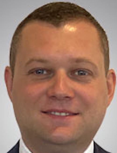
Mr. Thorsten Scheidler has been appointed managing director for Palomar Technologies' operations in Europe (HQ: Erlangen D), effective October 1, 2022. Mr. Scheidler replaces Mr. Josef Schmidl who is retiring after more than 30 years with Palomar Technologies. 

Thorsten Scheidler
“It’s with sad hearts that we announce the retirement of our long-time colleague, Mr. Josef Schmidl, yet welcome Mr. Scheidler to his new position as managing director for Palomar Europe,” said Bruce Hueners, President and CEO for Palomar Technologies, Inc. “We wish Mr. Schmidl a long, healthy and happy retirement and wish Mr. Scheidler great success in his new role and look forward to working with him.”

Over his 30+ years with Palomar Technologies, Mr. Schmidl was instrumental in opening up the European market to Palomar semiconductor packaging equipment and building the market. He joined Hughes Aircraft in 1986 as a service and applications engineer. In 1995, Mr. Schmidl moved to sales and two years later, he established Palomar GmbH in Erlangen, Germany, a wholly-owned subsidiary of Palomar Technologies. Since then, Mr. Schmidl has grown Palomar GmbH into an organization that provides sales and service support to customers in Europe, Russia, the Middle East, and Africa.

Mr. Thorsten Scheidler, Sales Director Europe for SST Vacuum Reflow Systems has over 15 years of sales and technical support experience within the power electronics and semiconductor industries in Europe. He has been instrumental in implementing sales strategies for Palomar’s wholly owned subsidiary, SST Vacuum Reflow Systems in the EMEA market.

@PalomarTech #Pauto #Europe

Wednesday, 20 July 2022

Innovation centre in Singapore.

Palomar Technologies, is expanding its Innovation Center in Singapore to meet a growing demand in Southeast Asia for process development and specialty OSAT for advance semiconductor new product introductions.

Palomar opened its Innovation Center – Singapore in November of 2018 to address a vital market need for process development, device package prototyping, test and measurement, process maturation, and low-volume production. In 2019, market demand pushed Palomar to make its first expansion. This second expansion gives the center the added ability to work closer with customers on their specific needs.

The Singapore Cntre currently supports a wide range of customer applications including:

  • Micro optics used in 3D Imaging, LIDAR and Optical Sensors
  • RF LDMOS and RF GaN power amplifiers
  • High-reliability RF Microwave modules
  • Silicon Photonics and laser diode placement bonding
  • Thermal and Motion Sensors
  • Optical transceiver packaging
  • Active Optical Cable packaging
  • VCSEL, EEL, EML, LED placement and bonding
  • Lens placement and lens attach bonding

“Strong demand from our regional Asia Pacific customer base has driven us to expand the footprint of our Singapore Innovation Center for the second time in five years,” said Rich Hueners, Managing Director, Palomar Technologies (SE Asia) Pte Ltd. “This expanded area will serve to host plasma cleaning, dry boxes and customer-specific test equipment while the original lab area will continue to host the die attach, wire bond and vacuum reflow equipment. We are looking forward to forging ahead with new customer requirements in this larger space.”

 @PalomarTech #PAuto #Packaging

Tuesday, 13 April 2021

Photonics and microelectronic device packaging.

Palomar Technologies are offering a webinar achieving die bonding flexibility for the next-generation of photonics packaging currently in development. (28th Apl 2021)

Much of the semiconductor packaging industry is engaged in an exciting and growing photonics ecosystem. Anticipating a seven percent CAGR over the next five years, this clearly outpaces most other manufacturing sectors. The associated challenges of photonics packaging, specifically relating to optical transceivers, include meeting anticipated performance gains while squeezing large package functionality into smaller, more thermally efficient footprints.

Palomar Technologies’ 3880 Die Bonder provides the flexibility and versatility to handle the many challenges present in both the current and next generation of photonics packaging. Not only is the 3880 capable of a diverse range of processes from epoxy dispense, to UV snap cure, to eutectic die attach, but can scale with production volume for low volume process development to full-scale high volume production. 

In this webinar, Kyle Schaefer, Palomar Product Marketing Manager reviews the challenges of photonics packaging and visits Live with Martyn Davies, New Business Development from Palomar Technologies UK, at the Palomar Demo Lab in the EPIC Center in Paignton (GB).  Martyn will provide a live overview of the Palomar 3880 capabilities for photonics packaging.

@PalomarTech #PAuto #Packaging